Vetiver oil has amber-brown color and it`s described as a sweet, woody and smoky fragrance that similar to patchouli oil and sandalwood Essential Oil, the odor of vetiver develops and improves with aging, and the scent varies depending on the plant`s location. Vetiver oil is known as a sacred herb valued because of its uplifting, soothing, healing and protective properties. It`s a natural body cooler that is also known as the 'oil of tranquility' because of its calming properties. It is a popular ingredient for soaps, toiletries and perfumes.
Vetiver Essential Oil,Natural Vetiver Essential Oil,Pure Vetiver Essential Oil,Organic Vetiver Essential Oil Xinhui Gangzhou Flavors&Fragrance Co.,Ltd , https://www.xhgzff.com
Introduction
The silicon wafer preparation process begins with a silicon single crystal rod and ends with a clean polished sheet to be used in an excellent environment. During this period, there are many processes and cleaning steps from a single crystal silicon rod to processing a number of wafers that meet special requirements. Except for many process steps, the entire process is almost always carried out in a dust-free environment. The processing of the wafer begins with a relatively dirty environment and is ultimately completed in a level 10 net vacancy. Process Overview All process steps are summarized into three main categories: ability to modify physical properties such as size, shape, flatness, or performance of some bulk materials; to reduce the amount of undesirable surface damage; or to eliminate surface contamination and Particles. The order of the process steps is important because the decision of these steps allows the wafer to be subjected to as little damage as possible and to reduce wafer contamination.
Table 1.1 Silicon wafer processing steps 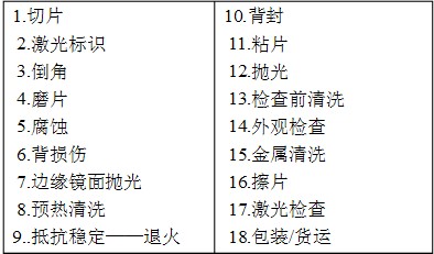
Slice (class 500k)
In the introduction of wafer processing, the first step from the single crystal silicon rod is to slice. The key to this step is how to minimize the loss when processing a single crystal silicon rod into a silicon wafer, that is, to process the single crystal rod as much as possible into a useful silicon wafer. In order to get the best silicon possible, the silicon requires a minimum amount of warpage and a minimum amount of knife loss.
There are two main ways in the slicing process - inner circle cutting and wire cutting. The reason these two forms of cutting are applied is that they minimize material loss, minimize damage to the wafer, and allow wafer warpage to be minimal.
Slicing is a relatively dirty process that can be described as a grinding process that produces large amounts of particles and a large amount of very shallow surface damage.
After the wafer is cut, the bonded carbon plate and the adhesive used to bond the carbon sheets must be removed from the wafer. In this cleaning and cleaning process, it is important to keep the order of the wafers because they are not yet distinguished by the logo.
Laser logo (Class 500k)
After the ingot is cut into a piece of silicon, the wafer is laser engraved. A high-power laser printer is used to engrave the surface of the wafer. The silicon wafers are encoded in the same order as they are cut from the ingot, so that the correct position of the wafer is known. This code should be uniform to identify the silicon chip and know its source. The code can indicate from which position of the single crystal rod the silicon wafer is cut. It is important to maintain such traceability because the overall properties of the single crystal will vary from one end of the ingot to the other. The number needs to be engraved deep enough to remain after the final wafer is polished. After engraving the code on the silicon chip, even if the silicon chip is missing, it can be traced back to the original position, and if the trend is clear, then the correct measures can be taken. The laser marking can be on the front side of the wafer or on the back side, although the front side is usually used.
Chamfer
When the wafer is finished, the wafer has sharp edges and needs to be chamfered to form a bullet-like smooth edge. The chamfered silicon wafer edge has a low center stress, which makes it stronger. The reinforcement of the edge of the wafer enables it to reduce the chipping of the wafer during subsequent wafer processing.
Grinding disc (Class 500k)
The next step is to remove the different damages that occur during the slicing process and laser marking, which is done during the grinding process. At the time of grinding, the silicon wafer is placed on the carrier and placed around some of the grinding discs. Both sides of the wafer can be in contact with the grinding disc so that both sides of the wafer can be ground simultaneously. The grinding disc is made of cast iron with a serrated edge. The upper disc has a series of holes that allow the sand to spread over the wafer and move with the mill. The grinding disc removes the serious damage caused by the slicing, leaving only a few balanced and shallow scars; the second benefit of the grinding disc is that after the grinding, the wafer is very flat because the disc is extremely flat.
The grinding process is mainly a mechanical process, and the grinding disc presses the grinding sand on the surface of the silicon wafer. The abrasive sand is composed of fine particles formed by retarding the calcination of the alumina solution, which can grind the outer layer of silicon. The depth of the outer layer being ground is deeper than the depth of the damage caused by the slice.
Corrosion (Class 100k)
After grinding, there is still a certain amount of equalized damage on the surface of the wafer, which is removed, but causes additional damage as low as possible. More distinctive is the use of chemical methods. There are two basic methods of corrosion: alkali corrosion and acid corrosion.
Back damage (Class 100k)
Mechanical damage is applied to the back side of the silicon wafer to form a metal gettering center. When the silicon wafer reaches a certain temperature, metal atoms such as Fe, Ni, Cr, Zn, etc., which reduce the carrier lifetime, move in the silicon body. When these atoms encounter damage points on the back side of the wafer, they are trapped and instinctively moved from the inside to the point of damage. The introduction of back damage is typically by impact or wear. For example, the impact method is sandblasted, and the wear is rubbed on the surface of the wafer with a brush.
Edge polishing
The purpose of wafer edge polishing is to remove etch pits remaining at the edge of the wafer. As the edge of the wafer becomes smooth, the stress at the edge of the wafer becomes uniform. The uniform distribution of stress makes the silicon wafer stronger. The polished edge minimizes the adsorption of particulate dust. The polishing method of the edge of the wafer is similar to the polishing of the surface of the wafer.
Preheating cleaning (Class 1k)
Before the silicon wafer enters the resistance, it needs to be cleaned to remove the organic matter and metal contamination. If the metal remains on the surface of the silicon wafer, it will enter the silicon body when it enters the stable process and the temperature rises. The cleaning process here is to immerse the silicon wafer in a cleaning solution (H2SO4+H2O2) capable of removing organic matter and oxides. Many metals are dissolved in the chemical cleaning solution as oxides; then, using hydrofluoric acid (HF) The oxide layer on the surface of the silicon wafer dissolves to remove dirt.
Resistance to stability - annealing (Class 1k)
The silicon wafer is grown in a high concentration oxygen atmosphere in the CZ furnace. Because most of the oxygen is inert, there is still a small amount of oxygen that forms small groups. These groups will act as n-donors, which will make the silicon's resistivity test incorrect. To prevent this from happening, the silicon wafer must first be heated to around 650 °C. This high temperature causes oxygen to form large groups without affecting resistivity. The wafer is then quenched to hinder the formation of small oxygen groups. This process can effectively eliminate the characteristics of oxygen as an n-donor and stabilize the true resistivity.
Back seal (Class 10k)
For heavily doped silicon wafers, a high temperature stage is applied to deposit a thin film on the backside of the silicon wafer to prevent outdiffusion of the dopant. This layer acts as a sealant to prevent the escape of dopants. Three types of films are commonly used as backfill materials: silicon dioxide (SiO2), silicon nitride (Si3N4), polysilicon. 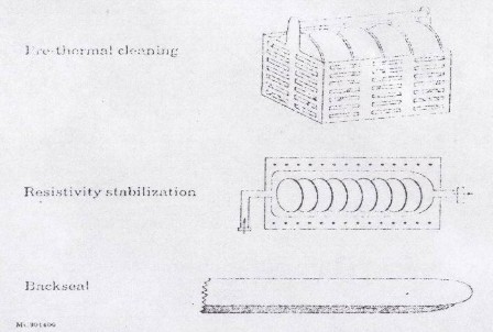
Before polishing, the adhesive sheet is first applied. The adhesive sheet must ensure that the wafer can be polished flat. There are two main methods of bonding, namely wax or stencil.
The wax paste is bonded to the wafer with a solid rosin wax and provides an extremely flat reference surface. This surface provides a solid reference plane for polishing. The viscous wax prevents the movement of the wafer as it is polished under a carrier on one side. Wax sheets are only useful for single-sided polished wafers.
Another method is the template adhesive, which has two different variations. One is only suitable for single-sided polishing. In this way, the silicon wafer is fixed on a circular template and placed on a soft liner. This pad provides sufficient friction so that when polishing, the edge of the wafer does not fully support the side carrier, and the wafer is not "hard" but "floating" on the object. When the front side is polished, the one-sided adhesive sheet protects the back side of the silicon wafer. Another method is suitable for double-sided polishing. This method allows for simultaneous polishing on both sides of a machine, similar to a grinding machine. The two polishing pads of the silicon wafer are placed in opposite directions so that the silicon wafer is pushed toward the top in one direction and the bottom in the opposite direction, and the stresses generated cancel each other out. This is advantageous in preventing the silicon wafer from being pushed toward the rigid carrier and causing damage to the edge of the wafer.
Polishing (Class ≤ 1k)
The purpose of wafer polishing is to obtain a silicon surface that is very smooth, flat, and free of any damage. When grinding a wafer, the silicon wafer is mechanically ground; while polishing, it is a chemical/mechanical process. This difference in operating principle is responsible for the polishing effect that results in a smoother surface than the abrasive sheet.
For polishing, the wafer is chemically/mechanically polished with a special polishing pad and special polishing sand. The polishing sand consists of silica gel and a special high pH chemical. This high pH chemical oxidizes the surface of the sheet and mechanically removes the oxide layer from the surface with a polishing sand containing silica gel.
Wafers are usually polished in multiple steps. The first step is a coarse throw, with a harder pad, the sand is more easily reacted with it, and there are more coarse silica particles in the sand used in the subsequent polishing. The first step is to remove corrosion spots and some mechanical damage. In the subsequent polishing, a soft lining, polishing sand containing less chemicals and fine silica particles was used. The final polishing to remove residual damage and mist is called fine polishing.
The adhesive sheet and polishing process are as shown: 
Cleaning before inspection (class 10)
After the wafer is polished, there is a large amount of contaminant on the surface. In order to be able to inspect the wafer, cleaning is required to remove most of the particles. Through this cleaning, the cleanliness of the silicon wafer still can not meet the customer's requirements, but it can be checked.
The usual cleaning method is to use RCA SC-1 cleaning solution after polishing. Sometimes it is more effective to use magnetic ultrasonic cleaning when cleaning with SC-1. Another method is to first wash with H2SO4/H2O2 and then with HF. In contrast, this method is more effective in removing metal contamination.
an examination
After polishing and cleaning, it can be inspected. In the inspection process, the resistivity, warpage, total thickness tolerance and flatness are tested. All of these measurement parameters are tested in a non-contact manner so that the polished surface is not damaged. At this point, the silicon wafer must ultimately meet the customer's dimensional performance requirements, otherwise it will be eliminated.
Metal removal cleaning
After the wafer is inspected, a final cleaning is performed to remove any particles remaining on the surface of the wafer. The main contaminant is the metal ions that remain on the surface of the wafer after cleaning. These metal ions come from various processes that use metal to contact with silicon wafers, such as slicing and grinding. Some metal ions are even derived from the chemicals used in the previous cleaning processes. Therefore, the final cleaning is mainly to remove metal ions remaining on the surface of the silicon wafer. The reason for this is that metal ions can cause minority carrier lifetimes, which can degrade device performance. The SC-1 standard cleaning solution is not very effective at removing metal ions. Therefore, it is necessary to use different cleaning solutions, such as HCl.
Wipe sheet
After cleaning the wafer with HCl, some particles may also be adsorbed on the surface. Some manufacturers choose brushes made of PVA to remove these residual particles. During the scrubbing process, pure water or ammonia (NH4OH) should flow through the surface of the wafer to carry away the adhering particles. Wiping the sheet with PVA is an effective means of removing particles.
Laser inspection
After the final cleaning of the wafer is completed, surface particles and surface defects need to be inspected. The laser inspection instrument detects particles and defects on the surface. Because the laser is a high-intensity wave source in short-wave. The laser is reflected on the surface of the wafer. If there is no problem with the surface, the light hits the surface of the wafer and reflects at the same angle. However, if light strikes the particle or hits a rough surface, the light will not reflect at the same angle. The reflected light travels in all directions and can be detected at different angles.
Packaging/freight
The purpose of the packaging is to provide a dust-free environment for the wafer and to protect the wafer from any damage during transport; the package also protects the wafer from moisture. If a good piece of silicon is placed in a container and contaminated, it will be as contaminated as any stage in the processing of the wafer, even considered to be a more serious problem because of wafer production. In the process, as each step is completed, the value of the wafer is also rising. The ideal packaging is to provide a clean environment while controlling the cleanliness of the small environment during storage and transportation. Typical shipping containers are made of polypropylene, polyethylene or some other plastic material. These plastics should not release any gas and are dust-free so that the surface of the wafer is not contaminated.
Silicon wafer preparation stage
Many parameters are involved in the fabrication of silicon wafers. And many of these parameters will change depending on the final silicon target. For silicon wafers, some parameters are always important, such as flatness, defects, contamination, etc.
When the wafer is cut by an incorrectly running blade, it creates a curved edge. These edges are not the same, which gives the wafer a different type of planar defect. Therefore, the silicon wafer should be cut as flat as possible.
There are different measurement methods to test the flatness of the wafer. The overall flatness is important for designing samples. On the other hand, local flatness is important for design. Some terms of overall flatness test are bow, warp. Total thickness tolerance (TTV), total indicator reading (TIR), and focal plane deviation (FPD). (To be continued)
Abstract In order to help everyone understand and understand the detailed production process of silicon materials to silicon wafers, and improve the understanding of this industry, in order to better engage in an industry, now some of the production process information is organized as follows, I hope to help everyone. . Introduction to the preparation process of silicon wafers from...
In order to help everyone understand and understand the detailed production process of silicon materials to silicon wafers, improve the awareness of this industry, in order to better engage in an industry, now some of the production process information is organized as follows, I hope to be helpful to everyone. The figure illustrates the steps of preheating cleaning, resistance to stabilization, and back sealing.
Adhesive sheet (Class 10k)